Semiconductor Electronics Materials Devices And Simple Circuits MCQ Class 12 Physics
Please refer to Chapter 14 Physics Class 12 MCQ Questions Semiconductor Electronics Materials Devices And Simple Circuits with answers below. These multiple-choice questions have been prepared based on the latest NCERT book for Class 12 Physics. Students should refer to MCQ Questions for Class 12 Physics with Answers to score more marks in Grade 12 Physics exams. Students should read the chapter Semiconductor Electronics Materials Devices And Simple Circuits and then attempt the following objective questions.
Chapter 14 Physics Class 12 MCQ Questions Semiconductor Electronics Materials Devices And Simple Circuits with answers
Chapter 14 Physics Class 12 MCQ Questions Semiconductor Electronics Materials Devices And Simple Circuits with answers provided below covers all important topics given in this chapter. These MCQs will help you to properly prepare for exams.
Question. In a semiconductor, the forbidden energy gap between the valence band and the conduction band is of the order of:
(a) 1 Mev
(b) 1 ev
(c) 0.1 Mev
(d) 5ev
Answer
B
Question. In reverse biasing:
(a) large amount of current flows
(b) no current flows
(c) potential barrier across junction increases
(d) depletion layer resistance increases
Answer
C
Question. To obtain electrons as majority charge carriers in a semiconductors the impurity mixed is:
(a) monovalent
(b) divalent
(c) trivalent
(d) pentavalent
Answer
B
Question. At absolute zero, Si acts as a
(a) metal
(b) semiconductor
(c) insulator
(d) none of these
Answer
C
Question. In semi conductor which are responsible for conduction:
(a) only electron
(b) electron and hole both
(c) only hole
(d) None of these
Answer
B
Question. Potential barrier developed in a junction diode opposes the flow of
(a) minority carrier in both regions only
(b) majority carriers only
(c) electrons in p region
(d) holes in p region
Answer
B
Question. In a p-type semiconductor, current conduction is by:
(a) atoms
(b) holes
(c) electrons
(d) protons
Answer
B
Question. Winch of the following gate is not an universal gate?
(a) OR
(b) NOT
(c) AND
(d) NAND
Answer
D
Question. In an n-type silicon, which of the following statements is true.
(a) Electrons are majority carriers and trivalent atoms are the dopants’
(b) Electrons are minority carriers and pentava- lent atoms are the dopants.
(c) Holes are minority carriers and pentavalent atoms are the dopants.
(d) Holes are majority carriers and trivalent atoms are the dopants.
Answer
C
Question. In a common base amplifier the phase difference between the input signal voltage and output voltage is :
(a) π/2
(b) 0
(c) π/4
(d) π
Answer
B
Question. Crystal diode is:
(a) amplifying device
(b) fluctuating device
(c) non-linear device
(d) linear device
Answer
C
Question. In a half wave rectifier circuit operating from 50 Hz mains frequency, the fundamental frequency in the ripple would be
(a) 25 Hz
(b) 50 Hz
(c) 70.7 Hz
(d) 100 Hz
Answer
B
Question. The energy band gap is maximum in which of the following?
(a) Metals
(b) Superconductors
(c) Insulators
(d) Semiconductors
Answer
C
Question. What is the number of possible crystal systems?
(a) 5
(b) 7
(c) 14
(d) 16
Answer
B
Question. If a small amount of antimony is added to germanium crystal
(a) its resistance is increased
(b) it becomes a p-type semiconductor
(c) there will be more free electrons than holes in the semiconductor,
(d) none of these.
Answer
C
Question. In good conducrors of electricity the type of bonding that exist is
(a) Van der Walls
(b) covalent
(c) ionic
(d) metallic
Answer
D
Question. Main function of a transistor is to :
(a) rectify
(b) simplify
(c) amplify
(d) all the above
Answer
C
Question. A p-type semiconductor is
(a) positively charged
(b) negatively charged
(c) uncharged
(d) uncharged at 0K but charged at higher temperatures
Answer
C
Question. If in a n-type semiconductor when all donor states are filled, then the net charge density in the donor states becomes
(a) 1
(b) > 1
(c) < 1, but not zero
(d) zero
Answer
B
Question. In a common base circuit, the current gain is 0.96. If the base current is 60μ A, the emitter current and collector current
(a) 2 mA
(b) 4 mA
(c) 2.2 mA
(d) 1.4 mA
Answer
D
Question. In a half wave rectifier, the r.m.s. value of the a.c. component of the wave is
(a) equal to d.c. value
(b) more than d.c. value
(c) less than d.c. value
(d) zero
Answer
B
Question. The impurity atoms with which pure silicon may be doped to make it a p-type semiconductor are those of
(a) phosphorus
(b) boron
(c) antimony
(d) nitrogen
Answer
B
Question. For the depletion region of a diode which one is incorrect?
(a) There are no mobile charges.
(b) Equal number of holes and electrons exists, making the region neutral.
(c) Recombination of holes and electrons has taken place.
(d) Immobile charged ions exist.
Answer
A
Question. Number of electrons in the valence shell of a pure semiconductor is
(a) 1
(b) 2
(c) 3
(d) 4
Answer
D
Question. The Voltage gain is highest for
(a) common emitter amplifier
(b) common base amplifier
(c) common collector amplifier.
(d) Equal in all the three.
Answer
A
Question. In principle, Boolean algerbra is based on:
(a) simple numbers
(b) binary numbers
(c) logic
(d) truth
Answer
C
Question. In the middle of the depletion layer of a reverse- biased p-n junction, the
(a) electric field is zero
(b) potential is maximum
(c) electric field is maximum
(d) potential is zero
Answer
C
Question. The forbidden energy gap for germanium crystal at 0 K is
(a) 0.071 eV
(b) 0.71 eV
(c) 2.57 eV
(d) 6.57 eV
Answer
B
Question. Region without free electrons and holes in a p-n junction is
(a) n-region
(b) p-region
(c) depletion region
(d) none of these
Answer
C
Question. In a p-type semiconductor, the acceptor valence band is
(a) close to the valence band of the host crystal
(b) close to conduction band of the host crystal
(c) below the conduction band of the host crystal
(d) above the conduction band of the host crystal
Answer
A
Question. In reverse biasing:
(a) large amount of current flows
(b) no current flows
(c) potential barrier across junction increases
(d) depletion layer resistance increases
Answer
C
Question. Filter circuit
(a) eliminates a.c. component
(b) eliminates d.c. component
(c) does not eliminate a.c. component
(d) None of these
Answer
A
Question. A p-n junction is fabricated from a semiconductor with band gap of 3.0 eV. The wavelength of the radiation which it can detect is
(a) 600 nm
(b) 400 nm
(c) Both of these
(d) None of these
Answer
B
Question. One serious drawback of semi-conductor devices is
(a) they do not last for long time.
(b) they are costly
(c) they cannot be used with high voltage.
(d) they pollute the environment.
Answer
C
Question. In a semiconductor
(a) there are no free electrons at 0 K
(b) there are no free electrons at any temperature
(c) the number of free electrons increases with pressure
(d) the number of free electrons is more than that in a conductor
Answer
A
Question. At absolute zero, Si acts as a
(a) metal
(b) semiconductor
(c) insulator
(d) none of these
Answer
C
Question. By increasing the temperature, the specific resistance of a conductor and a semiconductor
(a) increases for both
(b) decreases for both
(c) increases, decreases
(d) decreases, increases
Answer
C
Question. Bonds in a semiconductor :
(a) trivalent
(b) covalent
(c) bivalent
(d) monovalent
Answer
B
Question. The amount of photoelectric emission current depends on
(a) frequency of incident radiation
(b) intensity of incident radiation
(c) both frequency and intensity of incident radiation
(d) none of the above
Answer
B
Question. Diffusion current in a p-n junction is greater than the drift current in magnitude
(a) if the junction is forward-biased
(b) if the junction is reverse-biased
(c) if the junction is unbiased
(d) in no case
Answer
A
Question. A transistor is operated in common emitter configuration at VC = 2V such that a change in the base current from 100 mA to 300 mA produces a change in the collector current from 10mA to 20 mA. The current gain is
(a) 50
(b) 75
(c) 100
(d) 25
Answer
A
Question. In a n-type semiconductor, which of the following statement is true?
(a) Electrons are minority carriers and pentavalent atoms are dopants.
(b) Holes are minority carriers and pentavalent atoms are dopants.
(c) Holes are majority carriers and trivalent atoms are dopants.
(d) Electrons are majority carriers and trivalent atoms are dopants.
Answer
B
Question. The peak voltage in the output of a half-wave diode rectifier fed with a sinusoidal signal without filter is 10V. The d.c. component of the output voltage is
(a) 20/p V
(b) 10/Ö2 V
(c) 10/p V
(d) 10V
Answer
C
Question. If the ratio of the concentration of electrons to that of holes in a semiconductor is 7/5 and the ratio of currents is 7/4 then what is the ratio of their drift velocities?
(a) 5/8
(b) 4/5
(c) 5/4
(d) 4.7
Answer
C
Question. A solid that is not transparent to visible light and whose electrical conductivity increases with temperature is formed by
(a) ionic binding
(b) covalent binding
(c) metallic binding
(d) vander Waal’s binding
Answer
B
Question. In a transistor, the change in base current from 100 μA to 125 μA causes a change in collector current from 5 mA to 7.5 mA, keeping collector-to-emitter voltage constant at 10 V. What is the current gain of the transistor?
(a) 200
(b) 100
(c) 50
(d) 25.
Answer
B
Question. The circuit has two oppositively connected ideal diodes in parallel. What is the current flowing in the circuit?

(a) 1.71 A
(b) 2.00 A
(c) 2.31 A
(d) 1.33 A
Answer
B
Question. In a p-n junction photo cell, the value of the photoelectromotive force produced by monochromatic light is proportional to
(a) the voltage applied at the p-n junction
(b) the barrier voltage at the p-n junction
(c) the intensity of the light falling on the cell
(d) the frequency of the light falling on the cell
Answer
C
Question. The current gain β may be defined as
(a) the ratio of change in collector current to the change in emitter current for a constant collector voltage in a common base arrangement.
(b) the ratio of change in collector current to the change in the base current at constant collector voltage in a common emitter circuit
(c) the ratio of change in emitter current to the change in base current for constant emitter voltage in common emitter circuit.
(d) the ratio of change in base current to the change in collector current at constant collector voltage in common emitter circuit.
Answer
B
Question. The truth table given below is for
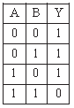
(a) NOR
(b) AND
(c) XOR
(d) NAND
Answer
D

We hope you liked the above Chapter 14 Physics Class 12 MCQ Questions Semiconductor Electronics Materials Devices And Simple Circuits with answers . In case you have any questions please put them in the comments box below and our teachers will provide you a response.